This case study employs a Socratic approach to encourage deeper engagement with the material. Rather than simply presenting solutions, the analysis is structured around probing questions that challenge you to think critically about the factors influencing semiconductor manufacturing performance. As you explore the data visualizations, you’ll encounter questions designed to challenge your assumptions, provoke thought, and guide you toward your own conclusions on optimizing yield and reducing defects.
1. Problem Statement
Despite high overall performance, certain shifts and process steps in semiconductor manufacturing show variability that leads to suboptimal yields and higher defect rates. Can these inefficiencies be addressed through data-driven strategies?
Key Questions to Explore
- What might be causing the Night Shift to consistently outperform other shifts in yield?
- Could the Evening Shift’s lower performance be linked to specific operational factors?
- How do environmental factors like temperature and pressure influence defect rates?
- Which process steps are most prone to variability, and how might they be stabilized?
2. Hypothesis
Consider these hypotheses:
- Could the practices of the Night Shift be identified and replicated to boost performance across other shifts?
- Is there a correlation between the lower yields of the Evening Shift and inconsistencies in process control?
- Might optimizing environmental conditions like temperature and pressure reduce defect rates, particularly in processes like Etching?
- Could focusing on the Etching process, which has higher defect rates, lead to overall process improvement?
3. Methodology
Data Acquisition:
The dataset comprises operational data from core manufacturing processes. How was the data been selected to be studied amongst other data?
Analytical Tools:
How can tools like Tableau and statistical analysis be used to uncover trends and correlations in this complex dataset?
Focus Areas:
In what ways might yield optimization and defect reduction strategies be identified through this analysis?
4. Data Analysis & Critical Questions
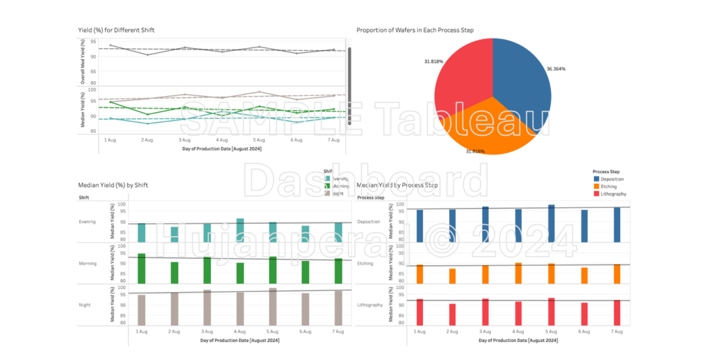
Dashboard consists of Yield (%) for Different Shift, Yield Analysis by Shift and Process Step (Bar Chart) and Wafer Distribution Across Process Steps (Pie Chart).

4.1 Line charts for Overall Yield and for Different Shifts
While the overall yield performance shows slight fluctuations, it remains generally stable. Does this indicate that the manufacturing plant’s yield is consistent? The Night Shift exhibits superior performance. What factors might contribute to this success, and could these practices be applied to improve yields during other shifts?
4.2 Wafer Distribution Across Process Steps (Pie Chart)
The distribution of wafers across processes appears even. What insights does this provide about process efficiency? Could it indicate areas of potential inefficiency that require further investigation?
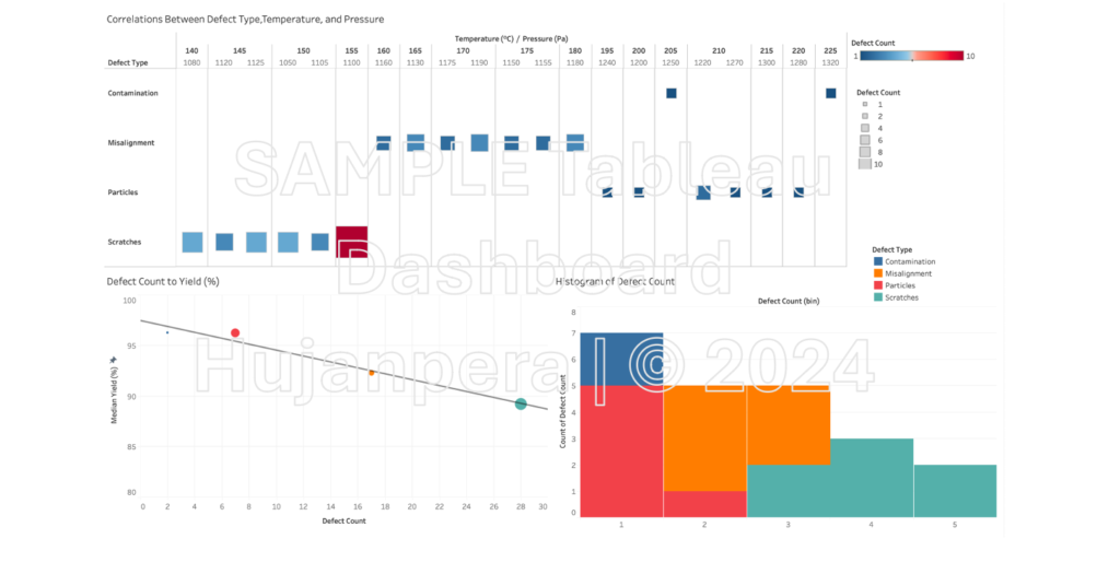
Dashboard of Defect Analysis consists of Heatmap Analysis of Correlation of Defect Type vs Environmental Factors, Correlation Between Defect Count to Yield and Defect Distribution Analysis (Histogram)

4.3 Heatmap Analysis of Defect Types vs. Environmental Factors
Certain defects correlate with higher temperatures and pressures. How might this relationship be understood? Does higher temperature always correlate with better yield, or could there be an optimal range that minimizes defects while maximizing yield?
4.4 Correlation Between Defect Count and Yield
There’s a strong inverse relationship between defect count and yield. What are the implications of this finding? If reducing defects is critical for maintaining high yields, what strategies could be most effective in achieving this?
4.5 Defect Distribution Analysis (Histogram)
Most wafers have 1-3 defects, with occasional spikes. What might be causing these spikes?Could these spikes in defect counts be tied to specific processes or conditions, and how might they be addressed?
5. Process Performance Analysis
While yield monitoring and defect analysis are vital in semiconductor manufacturing, they represent just a portion of the overall picture. A comprehensive understanding of process performance offers crucial insights into the manufacturing process itself, enabling a more integrated approach to ensuring quality and efficiency. By analyzing, optimizing, and controlling the core processes, semiconductor manufacturers can achieve higher yields, reduce defect rates, and produce superior products at a lower cost. In an industry where precision and quality are critical, process performance analysis is not just beneficial—it’s indispensable. As an exercise, outline the types of analyses needed and discuss how each can contribute to actionable insights.
Simplify Your Data, Empower Your Decisions with Custom Dashboards
At Hujanpera, we believe that data should work for you—not the other way around. Our custom dashboards transform complex data into clear, actionable insights that help you optimize processes and drive better results. Whether you’re managing semiconductor production or looking for ways to enhance your business efficiency, we’ll help you visualize the key metrics that matter most.
Why partner with Hujanpera?
- Clarity and Focus: Make sense of your data with streamlined, intuitive dashboards.
- Tailored Solutions: Every business is unique, and so are our solutions. We adapt to your needs.
- Better Decisions: Gain the confidence to make data-backed decisions that fuel growth and performance.
Ready to take control of your data? Visit our Contact Us page and let’s create a solution that fits your goals!